

2026-04-07

2026-04-03

2026-04-02

2026-04-01

2026-03-31

2026-03-24
Address: 3F , Blg 7 West, Sinosteel Building,Maque Industry Village Nanshan,Shenzhen,518057,Guangdong
Phone: +86-755-26971006
Mobile: 13751075276
Email: sales@acroview.com
There are many kinds of non-volatile storage elements, such as EPROM, EEPROM, NOR FLASH and NAND FLASH. The first two have been basically eliminated, so I only focus on the latter two. This article discusses the basic memory cell structure, write operation, The technology of erasing operation and read operation is briefly introduced, and the characteristics and application differences of NOR and NAND determined by the storage structure are introduced, and the subsequent hardware design and driver programming are pavement.
1 FLASH basic storage unit --- floating gate field effect tube
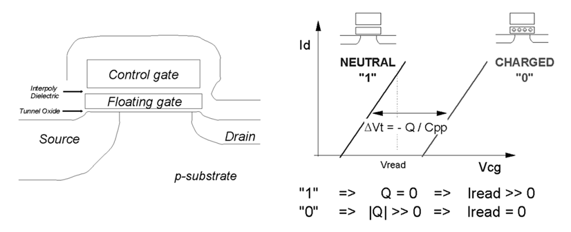
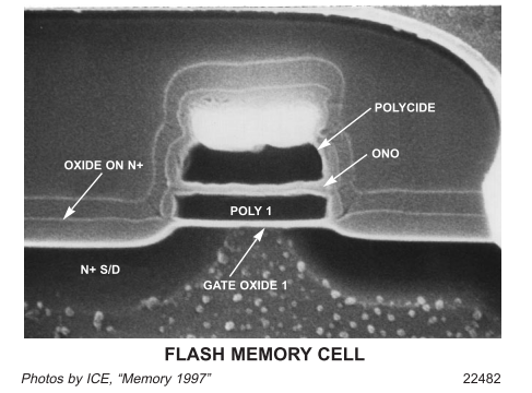
NOR FLASH and NAND FLASH both use floating gate FET (Floating Gate FET) as the basic storage unit to store data. The floating gate FET has 4 terminal electrodes, which are the source and drain ( Drain, Control Gate and Floating Gate. The first three terminal electrodes have the same effect on ordinary MOSFETs. The difference lies in the floating gate. FLASH is characterized by whether the floating gate stores charge or not. Numbers 0'and '1', when charges are injected into the floating gate, there is a conductive channel between D and S, read from D pole to '0'; when there is no charge in the floating gate, there is no conduction between D and S Channel, read from D pole to '1', the schematic diagram is shown in Figure 1.1 [1], Figure 1.2 is a cross-sectional view of an actual floating gate FET.
Note: SLC can be simply regarded as the use of whether the floating gate stores charge to characterize the numbers 0'and '1', while MLC uses the amount of charge in the floating gate to characterize '00', '01', '10' and ' 11', TLC is the same as MLC.
2 Operation of FLASH basic storage unit---write/erase/read
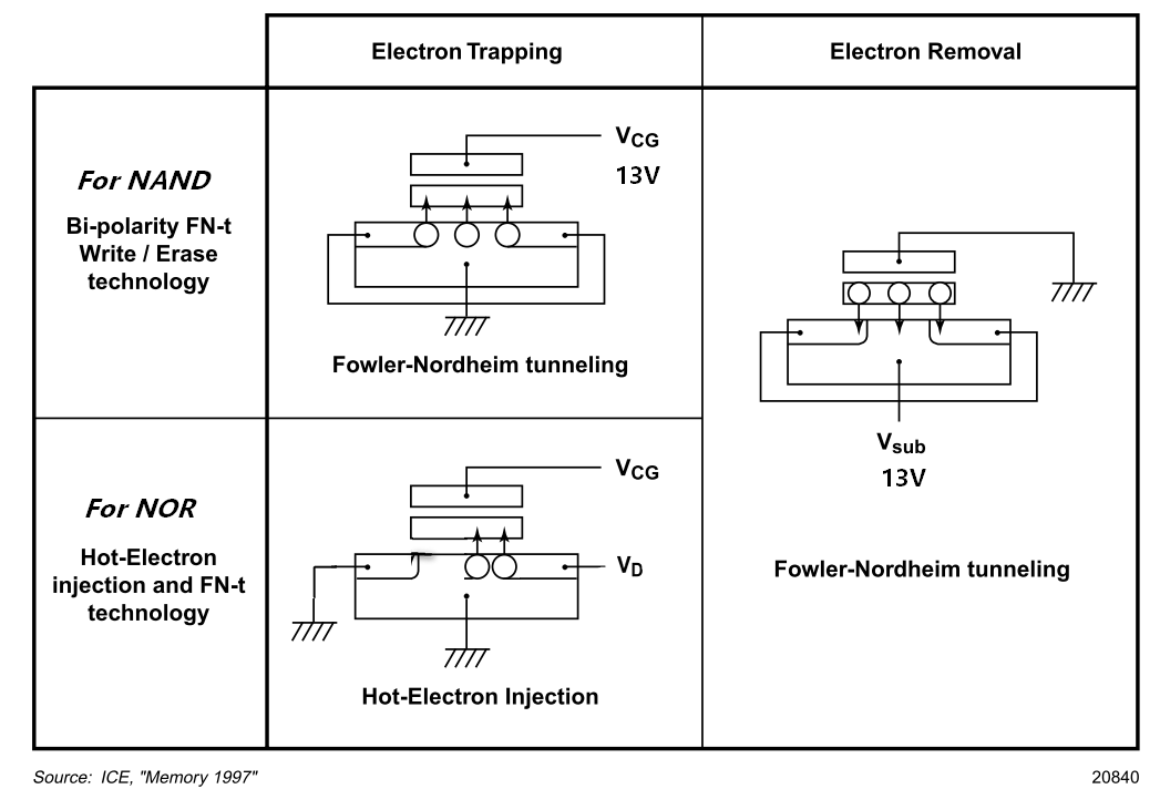
In FLASH, there are two commonly used techniques for injecting charges into the floating gate --- hot electron injection and FN tunneling (Fowler Nordheim tunneling); the technique for removing charges from the floating gate usually uses FN tunneling. (Fowler Nordheim tunneling), the basic principle is shown in Figure 2[2].
The write operation is the process of injecting charge into the floating gate. NOR FLASH injects charge into the floating gate through hot electron injection (this method has low charge injection efficiency, so the write rate of NOR FLASH is low), and NAND FLASH passes through the FN tunnel The effect injects charge into the floating gate. Before the FLASH write operation, the original data must be erased (that is, the charge in the floating gate is removed), that is, the readout after the FLASH is erased is ‘1’.
Erase operation is the process of removing the charge from the floating gate. Both NOR FLASH and NAND FLASH remove the charge from the floating gate through the F-N tunneling effect.
During the readout operation, the voltage applied to the control gate is very small and will not change the amount of charge in the floating gate, that is, the readout operation will not change the original data in the FLASH, that is, when the floating gate is charged, between D and S There is a conductive channel, read from D pole to '0'; when there is no charge in the floating gate, there is no conductive channel between D and S, and read from D pole to '1'.
3 Structure and characteristics of NOR FLASH and NAND FLASH
3.1 Structure and characteristics of NOR FLASH
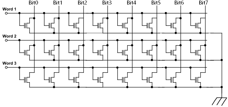
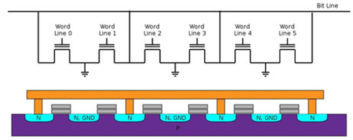
The schematic diagram of the NOR FLASH structure is shown in Figure 3.1. It can be seen that the basic storage units under each Bit Line are connected in parallel. When a Word Line is selected, the Word can be read, that is, the bit can be read. (I.e. Random Access), and has a higher reading rate, Figure 3.1 is a 3*8bit NOR FLASH principle structure diagram, Figure 3.2 is a cross-sectional view along the Bit Line section, showing a schematic diagram of the NOR FLASH silicon section. This parallel structure determines many characteristics of NOR FLASH.
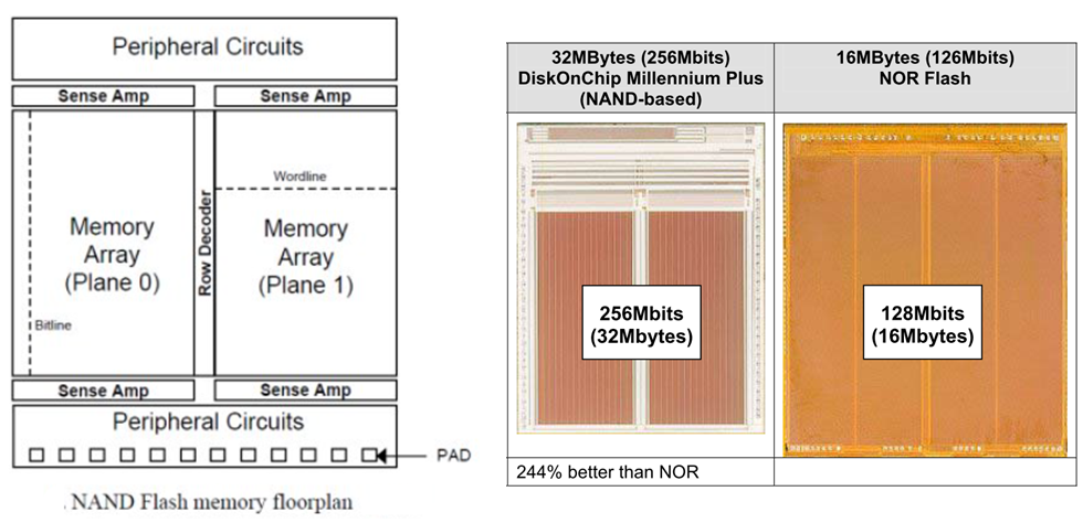
(1)基本存储单元的并联结构决定了金属导线占用很大的面积,因此NOR FLASH的存储密度较低,无法适用于需要大容量存储的应用场合,即适用于code-storage,不适用于data-storage,见图3.3[3]。
(2)基本存储单元的并联结构决定了NOR FLASH具有存储单元可独立寻址且读取效率高的特性,因此适用于code-storage,且程序可以直接在NOR 中运行(即具有RAM的特性)。
(3)NOR FLASH写入采用了热电子注入方式,效率较低,因此NOR写入速率较低,不适用于频繁擦除/写入场合。
最后来个小贴士:NOR FLASH的中的N是NOT,含义是Floating Gate中有电荷时,读出‘0’,无电荷时读出‘1’,是一种‘非’的逻辑;OR的含义是同一个Bit Line下的各个基本存储单元是并联的,是一种‘或’的逻辑,这就是NOR 的由来。
3.2 NAND FLASH的结构和特性
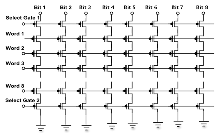
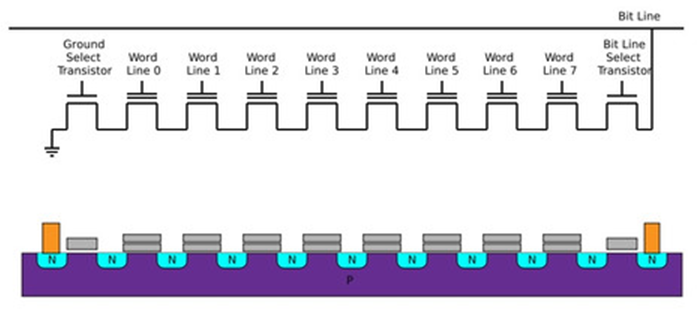
NAND FLASH的结构原理图见图3.4,可见每个Bit Line下的基本存储单元是串联的,NAND读取数据的单位是Page,当需要读取某个Page时,FLASH 控制器就不在这个Page的Word Line施加电压,而对其他所有Page的Word Line施加电压(电压值不能改变Floating Gate中电荷数量),让这些Page的所有基本存储单元的D和S导通,而我们要读取的Page的基本存储单元的D和S的导通/关断状态则取决于Floating Gate是否有电荷,有电荷时,Bit Line读出‘0’,无电荷Bit Line读出‘1’,实现了Page数据的读出,可见NAND无法实现位读取(即Random Access),程序代码也就无法在NAND上运行。
图3.4是一个8*8bit的NAND FLASH的原理结构图,图3.5是沿Bit Line切面的剖面图,展示了NAND FLASH的硅切面示意图,NAND FLASH的串联结构决定了其很多特点.
(1) The serial structure of the basic memory cell reduces the area occupied by the metal wire, and the utilization rate of Die is high. Therefore, the NAND FLASH storage density is high, and it is suitable for applications that require large-capacity storage, that is, suitable for data-storage, as shown in the figure. 3.3 [3].
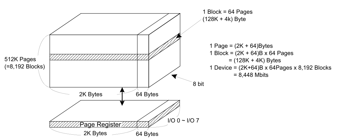
(2) The serial structure of the basic storage unit determines that NAND FLASH cannot be read by bit, and it cannot achieve independent addressing of the storage unit. Therefore, the program cannot run directly in NAND, so NAND uses Page as the reading unit and The writing unit, the block is the erase unit, as shown in Figure 3.6.
(3) NAND FLASH writing adopts F-N tunnel effect method, which has high efficiency, so the NAND erase/write rate is very high, which is suitable for frequent erasing/writing occasions. At the same time, NAND is read in pages, so the read rate is not low (slightly lower than NOR).
Finally, here is a tip: N in NAND FLASH is NOT, meaning that when there is a charge in the Floating Gate, read out '0', and when there is no charge, read out '1', which is a kind of'not' logic; The meaning of is that the basic memory cells under the same Bit Line are connected in series, which is a kind of "and" logic, which is the origin of NAND.
3.3 Comparison of NOR and NAND
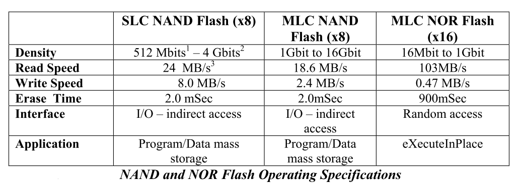
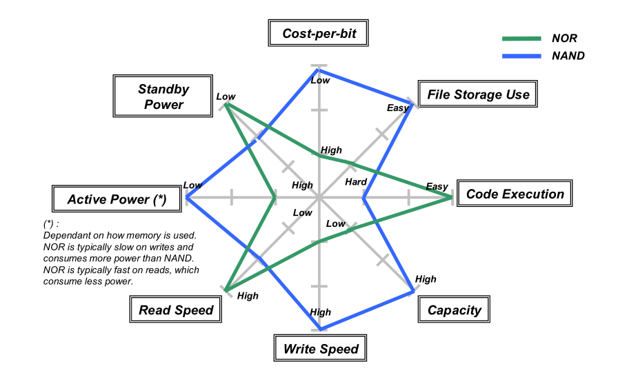
Through the analysis of the structure and characteristics of NOR and NAND in Sections 3.1 and 3.2, we can draw the conclusions in Figure 3.7 [5] and Figure 3.8 [5]. For a more detailed comparison, please refer to References [3]
4 Reliability of FLASH basic storage unit
The reliability of FLASH is beyond the scope of this article. If you are interested, please refer to References [7]
references
[1] Introduction to Flash Memory ROBERTO BEZ, EMILIO CAMERLENGHI, ALBERTO MODELLI, AND ANGELO VISCONTI
[2] FLASH MEMORY TECHNOLOGY
[3] Two Flash Technologies Compared: NOR vs NAND Written by: Arie Tal
[4] http://www.360doc.com/content/06/1120/10/12646_266138.shtml
[5] NAND vs. NOR Flash Memory Technology Overview TOSHIBA
[6] Flash Memory Cells—An Overview
[7] Reliability issues of flash memory cells
Remarks: transferred from CSDN
Last article:Comparison and difference between NorFlash, NandFlash and eMMC flash memory
Next article:Talking about SSD, eMMC, UFS

Dear, scan to add WeChat as a friend
Online Service
Phone

Top